- 您现在的位置:买卖IC网 > Sheet目录3872 > PIC18F45K20-I/PT (Microchip Technology)IC PIC MCU FLASH 16KX16 44TQFP
2009 Microchip Technology Inc.
Advance Information
DS41297F-page 27
PIC18F2XK20/4XK20
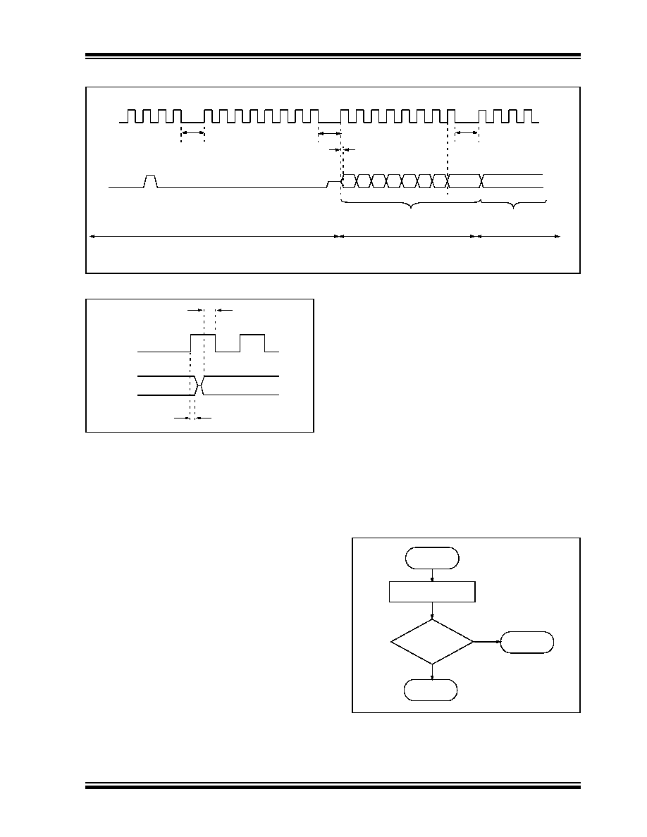
FIGURE 4-4:
SHIFT OUT DATA HOLDING REGISTER TIMING DIAGRAM (0010)
FIGURE 4-5:
HIGH-IMPEDANCE DELAY
4.5
Verify Data EEPROM
A data EEPROM address may be read via a sequence
of core instructions (4-bit command, ‘0000’) and then
output on PGD via the 4-bit command, ‘0010’ (TABLAT
register).
The
result
may
then
be
immediately
compared to the appropriate data in the programmer’s
memory for verification. Refer to Section 4.4 “Read
Data EEPROM Memory” for implementation details of
reading data EEPROM.
4.6
Blank Check
The term “Blank Check” means to verify that the device
has no programmed memory cells. All memories must
be verified: code memory, data EEPROM, ID locations
and Configuration bits. The device ID registers
(3FFFFEh:3FFFFFh) should be ignored.
A “blank” or “erased” memory cell will read as a ‘1’.
Therefore, Blank Checking a device merely means to
verify that all bytes read as FFh except the Configura-
tion bits. Unused (reserved) Configuration bits will read
‘0’ (programmed). Refer to Table 5-1 for blank configu-
ration expect data for the various PIC18F2XK20/
4XK20 devices.
Given that Blank Checking is merely code and data
EEPROM verification with FFh expect data, refer to
for implementation details.
FIGURE 4-6:
BLANK CHECK FLOW
12
3
4
PGC
P5
PGD
PGD = Input
Shift Data Out
P6
PGD = Output
56
7
8
1
23
4
P5A
910
11
13
15
16
14
12
Fetch Next 4-bit Command
01
0
PGD = Input
LSb
MSb
12
34
56
12
3
4
nn
n
P14
(Note 1)
Note
1:
Magnification of the High-Impedance delay between PGC and PGD is shown in Figure 4-5.
(Note 1)
MSb
nn
1
2
P19
PGD
PGC
P3
Yes
No
Start
Blank Check Device
Is
device
blank?
Continue
Abort
发布紧急采购,3分钟左右您将得到回复。
相关PDF资料
PIC16CR77-I/PT
IC PIC MCU 8KX14 44TQFP
PIC16F884-I/ML
IC PIC MCU FLASH 4KX14 44QFN
PIC16CR77-I/P
IC PIC MCU 8KX14 40DIP
PIC18F45K20-I/MV
MCU 32KB FLASH 1536B RAM 40-UQFN
PIC16CR76T-I/SS
IC PIC MCU 8KX14 28SSOP
PIC18F13K50-I/P
IC PIC MCU FLASH 4KX16 20-PDIP
PIC16CR76T-I/SO
IC PIC MCU 8KX14 28SOIC
PIC18LF24K22-I/MV
IC PIC MCU 16KB FLASH 28UQFN
相关代理商/技术参数
PIC18F45K20T-I/ML
功能描述:8位微控制器 -MCU 32KB Flash 1536B RAM 25 I/O 8B RoHS:否 制造商:Silicon Labs 核心:8051 处理器系列:C8051F39x 数据总线宽度:8 bit 最大时钟频率:50 MHz 程序存储器大小:16 KB 数据 RAM 大小:1 KB 片上 ADC:Yes 工作电源电压:1.8 V to 3.6 V 工作温度范围:- 40 C to + 105 C 封装 / 箱体:QFN-20 安装风格:SMD/SMT
PIC18F45K20T-I/MLV01
制造商:Microchip Technology Inc 功能描述:
PIC18F45K20T-I/MV
功能描述:8位微控制器 -MCU 32KB FL 1536b RAM 8b Familynanowatt XLP
RoHS:否 制造商:Silicon Labs 核心:8051 处理器系列:C8051F39x 数据总线宽度:8 bit 最大时钟频率:50 MHz 程序存储器大小:16 KB 数据 RAM 大小:1 KB 片上 ADC:Yes 工作电源电压:1.8 V to 3.6 V 工作温度范围:- 40 C to + 105 C 封装 / 箱体:QFN-20 安装风格:SMD/SMT
PIC18F45K20T-I/PT
功能描述:8位微控制器 -MCU 32KB Flash 1536B RAM 25 I/O 8B RoHS:否 制造商:Silicon Labs 核心:8051 处理器系列:C8051F39x 数据总线宽度:8 bit 最大时钟频率:50 MHz 程序存储器大小:16 KB 数据 RAM 大小:1 KB 片上 ADC:Yes 工作电源电压:1.8 V to 3.6 V 工作温度范围:- 40 C to + 105 C 封装 / 箱体:QFN-20 安装风格:SMD/SMT
PIC18F45K22-E/ML
功能描述:8位微控制器 -MCU 32KB Flash 1536B RAM 8B nanoWatt RoHS:否 制造商:Silicon Labs 核心:8051 处理器系列:C8051F39x 数据总线宽度:8 bit 最大时钟频率:50 MHz 程序存储器大小:16 KB 数据 RAM 大小:1 KB 片上 ADC:Yes 工作电源电压:1.8 V to 3.6 V 工作温度范围:- 40 C to + 105 C 封装 / 箱体:QFN-20 安装风格:SMD/SMT
PIC18F45K22-E/MV
功能描述:8位微控制器 -MCU 32KB 1536b RAM 8bit familynanoWatt XLP RoHS:否 制造商:Silicon Labs 核心:8051 处理器系列:C8051F39x 数据总线宽度:8 bit 最大时钟频率:50 MHz 程序存储器大小:16 KB 数据 RAM 大小:1 KB 片上 ADC:Yes 工作电源电压:1.8 V to 3.6 V 工作温度范围:- 40 C to + 105 C 封装 / 箱体:QFN-20 安装风格:SMD/SMT
PIC18F45K22-E/P
功能描述:8位微控制器 -MCU 32KB 1536bytes-RAM 8B nanoWatt RoHS:否 制造商:Silicon Labs 核心:8051 处理器系列:C8051F39x 数据总线宽度:8 bit 最大时钟频率:50 MHz 程序存储器大小:16 KB 数据 RAM 大小:1 KB 片上 ADC:Yes 工作电源电压:1.8 V to 3.6 V 工作温度范围:- 40 C to + 105 C 封装 / 箱体:QFN-20 安装风格:SMD/SMT
PIC18F45K22-E/PT
功能描述:8位微控制器 -MCU 32KB Flash 1536B RAM 8B nanoWatt RoHS:否 制造商:Silicon Labs 核心:8051 处理器系列:C8051F39x 数据总线宽度:8 bit 最大时钟频率:50 MHz 程序存储器大小:16 KB 数据 RAM 大小:1 KB 片上 ADC:Yes 工作电源电压:1.8 V to 3.6 V 工作温度范围:- 40 C to + 105 C 封装 / 箱体:QFN-20 安装风格:SMD/SMT